


Abstract
W and W–H complexes on graphene on Ir(111) were studied by means of low temperature scanning tunneling microscopy. H is found to coadsorb at the sample surface during W evaporation. Five different W-related structures on graphene on Ir(111) were found and characterized. They are identified as WHn, with  , as shown by electric field induced dehydrogenation. They exhibit a number of peculiar effects, such as electric field induced shifts of spectroscopic features as well as reversible switching and charging effects. In addition, two different structures of H on Ir(111) were characterized.
Export citation and abstract BibTeX RIS

Content from this work may be used under the terms of the Creative Commons Attribution 3.0 licence. Any further distribution of this work must maintain attribution to the author(s) and the title of the work, journal citation and DOI.
1. Introduction
The interaction of graphene with single atomic adsorbates is predicted to lead to a number of intriguing effects. For example, due to the absence of d-states in graphene, transition metal atoms adsorbed on graphene should exhibit large magnetic moments, which are often quenched on metallic substrates [1, 2]. However, these systems appear to be very complex and a number of calculations disagree about their properties. For example, the preferred adsorption site of Co on graphene was first calculated to be the center of a C hexagon [3], whereas calculations including a large local Coulomb repulsion suggested adsorption on top of a C atom with a different spin-state [4]. Furthermore, it was suggested that there could be different stable electronic configurations even in a single adsorption site for this system [5, 6].
The properties of transition metal adatoms on graphene are predicted to strongly depend on a number of external factors, such as electric fields [1], strain in the graphene sheet [7], doping of graphene [8, 9] or even the presence of a scanning tunneling microscopy (STM) tip [10]. A magnetic impurity on graphene is an interesting model system for investigating the Kondo effect [3, 11], since graphene has a unique electronic structure, the Fermi level can be shifted by applying an electric field and the symmetry of the system can be changed by a change of the adsorption site of the impurity [12, 13].
Possibly due to this complexity and the accompanying difficulties in the interpretation of experimental results, rather few experimental studies have been published. An STM study of Co on graphene has shown vibrational features and a charging of the adatoms [14]. Two different adsorption sites on graphene on H passivated SiC have been reported both for Ni and Co [15]. While Co seems to have different electronic configurations depending on the adsorption site and could be influenced by STM manipulation, Ni has the same electronic configuration in different adsorption sites and could not be manipulated. While Ni adatoms show no magnetic moment in x-ray magnetic circular dichroism experiments, Co and Fe adatoms do [16]. Recently, another STM study of Co adsorbed on graphene on Pt(111) showed adsorption strictly at graphene hollow sites [17]. The single Co atoms exhibit a magnetic anisotropy of ≈8 meV, an out-of-plane hard axis and a magnetic moment of 2.2 . The magnetic fingerprint in scanning tunneling spectroscopy (STS) spectra was attributed to inelastic spin-flip excitations. It was also shown that the Co atoms have a strong affinity towards hydrogenation. CoHn structures (
 ), which could be dehydrogenated with the STM, showed different magnetic properties. The affinity to hydrogen of single transition metal adatoms on surfaces has been shown previously and can lead to vibrational [18] or Kondo features [19] in STS experiments, depending on the system under consideration.
W on graphene has been predicted to show a large magnetic anisotropy and an easy axis of the magnetic moment that can be switched between in-plane and out-of-plane by an external electric field [1].
Here, we study W on graphene on Ir(111) with low temperature STM. As explained in section 2, W was evaporated from a resistively heated filament and, as it turned out, H was coevaporated, which is a known effect for hot W filaments [18]. In section 3, we first demonstrate the presence of H using observations of a line-pattern on the Ir(111) surface in low voltage STM topographs. Five different species of W or W–H complexes were observed and characterized (section 4). Although W–H complexes of each species share characteristic features that were used to characterize them, some other, more subtle properties differed from complex to complex. We observed that switching between the different structures was possible in a particular sequence, which is interpreted in terms of hydrogen desorption, while the reverse process, rehydrogeneation, occurred randomly.
2. Experimental details
Ir(111) surfaces were cleaned by cycles of Ar+-ion bombardment and subsequent annealing at ≈1600 K under ultra high vacuum (UHV) conditions. Hydrogen was adsorbed at a sample temperature of ≈35 K by introducing high purity H2 into the UHV system at partial pressures well below  Pa. For the work presented in section 4, graphene was grown on Ir(111) by room temperature adsorption of C2H4 (5 L, 1 L ≈133 × 10−6 Pa s) at the clean Ir(111) surface and subsequent annealing at ≈1400 K. This procedure leads to the formation of highly ordered graphene islands [20]. W was evaporated from a resistively heated filament onto the sample, which was kept at a temperature of below 12 K. Au and Ni tips were prepared by ex situ electrochemical etching and in vacuo annealing and Ar+-ion bombardment. The experiments of section 4 were performed with both Au and magnetized Ni tips. Since the features in the differential conductance spectra of W–H complexes of the same class scattered between individual complexes, an influence of the magnetization of the tip on the experimental results could not be identified.
  spectra and maps (I: current, V: sample voltage) were recorded by standard lock-in techniques with a typical modulation frequency of fmod = 7.2 kHz and a root mean square modulation amplitude of Vmod = 5 mV unless stated otherwise in the figure caption.
3. Hydrogen on Ir(111)
The adsorption of H on metal surfaces is a prototypical catalytic reaction, which has been studied for various metal surfaces since the 1970s [21]. On the Ir(111) surface, H2 adsorbs dissociatively [22]. The binding energy of H on the Ir(111) surface does not vary drastically with the adsorption site and correspondingly H is delocalized at low coverages at 90 K [22, 23]. At increasing coverages  H localizes in atop positions of the Ir(111) lattice [22].
When investigating W on graphene islands, we observed striped structures on the Ir substrate. To verify that these patterns are H-induced, we exposed clean Ir(111) at low temperatures (35 K) to up to 1 L of H2. The formation of two different structures depending on the hydrogen coverage was found. For low coverages ( L), most of the surface was clean and
  spectra showed a step-like feature at ≈−350 mV, indicative of an Ir(111) surface resonance [24]. At narrow terraces, a line-like pattern as shown in figure 1(a) was observed. In these regions the signature of the surface resonance was absent, as expected in the presence of adsorbates. A comparison to atomically resolved STM topographs of graphene on Ir(111) (not shown) yields that the line-pattern is oriented along the
  directions of the Ir(111) surface. The pattern is visible in the STM topographs at low voltages (
 mV). Tunneling at higher voltages (e.g., 1 V) or at large currents (e.g., when contacting the surface with the STM tip at low voltages) leads to changes of the pattern as illustrated in the inset of figure 1(a).
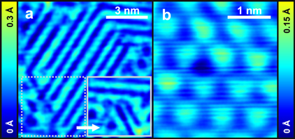
Figure 1. Low-pass filtered STM topographs of H on Ir(111). (a) Low coverage,  mV, I = 100 pA. Depression lines are observed along
  directions of the substrate and separated by either two or three Ir lattice rows (see supplementary data). The line-structure may be changed by tunneling at higher voltages or currents. The inset (gray rectangle) shows the area marked by the gray dotted rectangle, imaged after a scan at 1 V. The line-pattern changed drastically. (b) High coverage, V = 50 mV, I = 100 pA. A hexagonal pattern corresponding to a 3 × 3 superstructure is observed (see supplementary data).
Download figure:
Standard image High-resolution imageAt higher H2 exposure (e.g., 1 L), regions with a hexagonal pattern (see figure 1(b)) are observed in addition to the line pattern mentioned above. Like the latter one, the hexagonal structure can easily be modified by the STM tip. Atomistic models of the observed structures and a more detailed description of the STM induced modifications are presented in the supplementary data.
4. W and WH on graphene on Ir(111)

After the deposition of W, a line pattern in the low voltage STM topographs emerged, as illustrated in figure 2(a). As shown above, this indicates the presence of H on the surface1
. Figure 2(b) shows a series of STM topographs of a graphene island on Ir(111) after W deposition. Protrusions of different apparent heights and shapes are observed on the island. Based on these characteristics and  spectra (see the following subsections), the structures can be categorized into five different classes labeled A, B, C, D1 and D2, as indicated in figure 2(b).
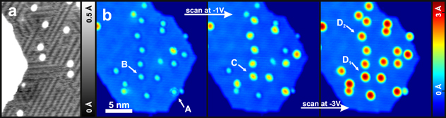
Figure 2. (a) STM topograph of the Ir(111) surface after deposition of W, V = −250 mV, I = 100 pA. The contrast is adjusted to show the line-structure, indicating the presence of H (see section 3). The white structure on the left hand side is the border of the graphene island shown in (b). (b) Series of STM topographs of a graphene island on Ir(111) after the deposition of W, V = −250 mV, I = 100 pA. Between the acquisition of the left and the middle image the area was scanned at a voltage of V = −1 V and at V = −3 V between the acquisition of the middle and the right image. The shapes and apparent heights of the W related structures changed during the higher voltage scans. They can be categorized into the indicated classes A, B, C, D1 and D2.
Download figure:
Standard image High-resolution imageThe W-related structures exhibited changes during STM imaging at elevated bias. For example, between the acquisition of the left and the middle images in figure 2(b), which were both recorded at  mV, the area was scanned at
  V. As a result, almost all W related structures changed their apparent heights and shapes. Between the acquisition of the middle and the right image the area was scanned at a voltage of V = −3 V and the W structures changed again.
From an analysis of many manipulation experiments we found that any structure from the above list may be switched to a subsequent one by applying a suitable voltage. E.g., structure A could be switched to any other structure, while no controlled conversion of structures D1 and D2 to any of their predecessors was possible. However, reversed processes (i.e., backwards in the list) were observed to happen randomly. Since H was present on the surface, this switching behavior can be explained as follows. Transitions from left to right reflect the removal of H from W under the influence of the electric field of the STM tip. The reverse process is consistent with the random attachment of diffusing hydrogen.
We discard the possibility that the clusters contain more than one W atom for the following reasons: if W atoms formed clusters on graphene, different series WHn, W2Hn, ... of complexes should be present. However, only a single series (A to D1/D2) was observed. Almost all observed complexes belonged to this series. Additionally, the size of complex D1, which appears largest in STM topographs, is close to that of single Co and Ni atoms on graphene [15].
Below, experimental results on the different structures are presented and suggestions for possible compositions are given, followed by a more detailed study of the conditions required to induce switching processes.
4.1. Structures D1 and D2
D1 is the structure that appears largest in STM topographs with an apparent height of ≈3.5 Å at  mV. Figure 3(a) shows a typical
  spectrum acquired above D1 with a pronounced peak labeled α at ≈100 mV. The position of peak α varied between 0 mV and 150 mV from structure to structure. No clear dependence of the peak position on external parameters, such as the position within the moiré unit cell or the distance to neighboring adsorbates or defects in the graphene sheet, was found. However, a peak in this energy window is consistent with the calculated density of state with
  -character for clean W on graphene [1]. The calculated electronic structure of this system appears to be very sensitive to the electric field, spin–orbit coupling and the magnetization direction [1]. Thus, subtle external influences that may not be obvious in our experiment may have a significant influence on the system. Indeed, as shown in figure 3(c), the energy of peak α of an individual D1 structure depends on the tip–sample distance, which was varied by changing the stabilizing current of the feedback loop at the start of the recording of the spectrum. The onset of the peak (defined as the voltage at which the
  signal has reached half of the peak amplitude) shifts linearly with the logarithm of the stabilizing current, i.e., the tip–sample distance. A similar effect has been shown for the electric field induced shifting of noble metal surface states, explained by the Stark effect [25, 26]. Double barrier tunneling through decoupled molecules on surfaces also leads to electric field induced shifting of features in
  spectra [27].
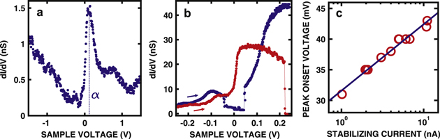
Figure 3. (a)  spectrum acquired at a D1 structure (Vmod = 15 mV). It shows a peak labeled α at V ≈140 mV. (b)
  spectra of two D1 structures, recorded from negative to positive sample voltage. The onset of the peak labeled α in (a) varied from structure to structure and usually occurred between ≈−30 mV and ≈150 mV. The blue curve shows a reversible switching to a state with lower differential conductance for voltages
  mV. This behavior was observed in a few cases. The red curve shows a sudden drop in the differential conductance close to V = 200 mV at a current of I ≈7 nA. As validated by subsequent imaging, such a sudden drop is due to a movement of the D1 structure away from the tip. (c) Onset voltages of the peak α, extracted from
  spectra of the same D1 structure at different tip–sample distances. The onset shifts linearly with the logarithm of the stabilizing current, i.e., the tip–sample distance.
Download figure:
Standard image High-resolution imageAdditional remarkable effects were found for the D1 structure. A reversible switching to a lower conductance state at voltages  mV was seen in some cases, as displayed in figure 3(b) (blue curve) by jumps in the differential conductance. Such jumps appear at random voltages within this window and are more common when peak α is farther away from the Fermi energy. Imaging of the structure before and after the acquisition of such a spectrum showed no difference. Another type of sudden change in the differential conductance (see figure 3(b), red curve) was accompanied by a lateral displacement of the atom, indicating a weak coupling to the substrate. This kind of STM induced movement of the D1 structure very often happened at voltages of V ≈ 200 mV. Assuming a tip–sample distance of 4 Å, this corresponds to an electric field of 50 mVÅ−1. Interestingly, at this electric field, a switching of the magnetic easy axis of W on graphene between in-plane and out-of-plane was predicted [1].
Structure D2 shows an apparent height of ≈2.7 Å at V = −250 mV.  spectra acquired at D2 structures show a pronounced narrow peak at or near the Fermi level (figure 4(a)). The energy of this resonance was observed to vary from structure to structure but the spectra were reproducible and independent of the tip–sample distance for each individual structure. Figure 3(b) shows a histogram of the resonance energies. While the resonance frequently occurred at the Fermi energy, voltages between −60 mV and 20 mV have been observed along with some scatter of the shape of the resonance. As for peak α of structure D1, the scatter of the resonance energy and shape indicates a strong influence of subtle external parameters.
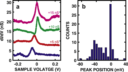
Figure 4. (a)  spectra acquired at D2 structures showing a peak close to the Fermi energy (V = 0 V). For clarity, the spectra have been vertically offset as indicated. (b) Histogram of the peak positions. While the most frequent position is V = 0 V, the values scatter between −60 mV and 20 mV.
Download figure:
Standard image High-resolution imageD type structures did not undergo transformations to any other structure within the parameter range of the experiments,  V, I
V, I  100 nA. At high currents (typically
  nA), the structures sometimes moved on the surface. In a few cases this was accompanied by switching between the two D structures. These observations indicate that D1 and D2 correspond to clean W without H. Different adsorption positions or electronic states of the adsorbed W, similar to the different states of Ni and Co on graphene [15], are the most likely explanation of the differences between D1 and D2.
Owing to the reported variability of the experimental data an unambiguous assignment of the D2 resonance is difficult. Possible interpretations are a Kondo effect or a W induced Dirac point resonance state of graphene, as suggested for Co on graphene [8].
4.2. Structure C
Structure C appears as elongated protrusion with a height of ≈2.4 Å in STM topographs at V = −250 mV (figures 2(b) (middle) and 5(a)). As shown in figure 5(a), the long axis is rotated by 30° with respect to straight borders of the graphene island, which are oriented along zig-zag directions of graphene [28]. This implies that structure C is elongated along the directions of the graphene C–C bonds. In  maps (e.g., at
  mV, see figure 5(b)) structure C is two-fold symmetric and exhibits a depression along the long axis. Figure 5(c) shows a STM topograph of three C structures recorded at V = −100 mV. They appear fuzzy, which can be interpreted as switching between different conformational or electronic states. This behavior can also be observed in
  spectra (figure 5(d)), where
  jumps between different levels at sample voltages below
  ≈150 mV.
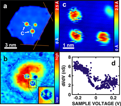
Figure 5. (a) STM topograph of W structures on a graphene island (V = −230 mV, I = 1 nA). The marked structures C are elongated along axes (white lines) which are rotated by 30° with respect to the borders of the graphene island (orange lines). (b) Map of  recorded simultaneously with (a) (Vmod = 10 mV). The
  patterns of C structures show two-fold symmetry with a central depression in direction of their elongation in the topograph (white lines). The background
  signal of the graphene island is due to a confined Ir(111) surface resonance [24]. (c) STM topograph of C structures on graphene (V = −100 mV, I = 100 pA). The lower left structure is the one marked C in figure 2(b). The structures appear fuzzy at sample voltages below
  mV, indicating switching processes. (d)
  spectrum acquired at a C structure. Jumps of
  at low voltages indicate an unstable tunneling junction, in line with unstable topographs at low voltage, as shown in (c).
Download figure:
Standard image High-resolution imageStructure C could be switched controlably to the D structures. This suggests that structure C comprises at least one H. A possible explanation for the fuzzy appearance in low voltage topographs is tip induced conformational switching of the complex, i.e., a movement of the H atom. The two-fold symmetry would also be consistent with the presence of two H atoms. In that case a switching to a different tip stabilized conformation at low voltages might occur, similar to the case of Ce, La and Cr on Ag(100) [18].
The most probable adsorption site for the W atom is the bridge site atop a graphene C–C bond since it provides two equivalent sites for the attached H, either along or perpendicular to the C–C bond direction. Other possible adsorption sites like top (atop a C atom) and hollow (at the center of a graphene honeycomb) exhibit three or six-fold symmetry with respect to graphene and are therefore incompatible with the observed two-fold symmetry.
4.3. Structure B
B structures display an apparent height of ≈0.8 Å in STM topographs recorded at V = −250 mV. They appear as round protrusions and are in some cases surrounded by a ring-shaped depression (figures 2(b), left and 6(a)). Figure 6(c) shows  spectra obtained at two different B structures. In contrast to all other structures, their spectra do not show any prominent features. Figure 6(b) shows a
  map recorded simultaneously with the topograph shown in figure 6(a). The
  signal observed on clean graphene is due to an Ir(111) surface resonance [24], which gets scattered at the borders of the graphene island, leading to a gradual suppression of the signal toward the edges. The C and D2 structures (higher structures on the left hand side) cause a depression of the
  signal that is restricted to their topographic extent. This indicates that they do not cause scattering of the surface resonance in the underlying substrate. In contrast, the B structures on the right hand side of the image cause depressions of
  which are much wider than their topographic footprints. This indicates a substantial scattering of the Ir surface resonance, similar to the scattering at the graphene edges. The small apparent size and the scattering properties indicate that B structures interact more strongly with the substrate than the other structures. Since it is possible to switch B structures to C, they contain at least one H atom more than structure C. Depending on the composition of C, structure B can be identified as WH2 or WH3.
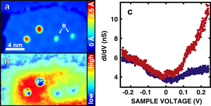
Figure 6. (a) STM topograph of W structures on a graphene island (V = −200 mV, I = 0.5 nA). The marked structures on the right are of type B. (b) Map of  recorded simultaneously with (a) (Vmod = 10 mV). The background
  signal of the graphene island is due to a confined Ir(111) surface resonance [24]. The small B structures in (a) cause wide depressions in the
  signal, compared to those of the larger structures on the left hand side. (c) Spectra of
  acquired at dfferent B structures (Vmod = 10 mV). Compared to
  spectra of structures of other types, they appear featureless.
Download figure:
Standard image High-resolution image4.4. Structure A
The appearance of structure A in STM topographs strongly depends on the tunneling voltage and the specific STM tip as well as the individual complex. Their defining feature is that STM topographs recorded at voltages between −200 mV and −400 mV show an abrupt change in the image when the tip comes close to the center of the structure, as shown in figure 7(a). When the lateral separation between the tip and the center of the structure is larger, the structure is in a state that appears large in the topograph and whose borders are imaged. When the tip comes closer, the structure switches reversibly to a state that appears smaller in the STM topograph. Figure 7(b) shows a  map recorded simultaneously with figure 7(a). A ring-like depression is observed at those locations where the topograph reveals the apparent switching of the structure. Increasing the negative voltage leads to an increase of the diameter of the ring. This behavior can best be seen from figure 7(e). It shows a number of colorcoded
  spectra, recorded along the green line shown in figure 7(d). A single
  spectrum corresponds to a horizontal cut in the map2
, while a
spectrum corresponds to a horizontal cut in the map2
, while a  map corresponds to a vertical cut. The switching effect can be seen as a blue (depression) parabola in this representation. Such a behavior is known from electric field induced charging of donors in semiconductors [29, 30] or molecules on surfaces [31, 32]. When the electric field at the position of the structure exceeds a certain value the structure gets charged and the tunneling current is affected. This defines the radius of a circle in the
  map.
map.

Figure 7. (a) STM topograph of a type A structure, recorded at V = −200 mV and I = 1 nA, showing drastic variations of the apparent height on a subatomic lateral scale. As the STM tip approaches to a certain distance from the center the structure switches to a different state that appears smaller. (b) Map of  recorded simultaneously with (a) (Vmod = 10 mV). A ring shaped depression at the location where the switching is observed in (a) is discernible. (c) Topograph of the structure from (a), recorded at V = −40 mV and I = 1 nA. The very symmetric type A complex has a cross-like appearance. (d) Map of
  acquired simultaneously with (c) (Vmod = 10 mV), showing distinct features with almost four-fold symmetry. (e) Color-coded
  spectra recorded along the green line in (a), where the red cross marks zero distance. (f)
  spectra recorded at the positions depicted in (a) by correspondingly colored crosses.
Download figure:
Standard image High-resolution imageThe most symmetric type A complexes appear like a cross at low negative voltages (figure 7(c), V = −40 mV). Figure 7(d) shows a  map recorded simultaneously with the topograph of figure 7(c). There are distinct features which are close to four-fold symmetric.
Since structure A can be switched to all other structures and it appears more frequently at higher H coverages, it contains more H atoms than the other structures. The (almost) four-fold symmetry of some type A complexes in the topographs and  maps tentatively suggests the presence of 4 H atoms in the structure, rendering it to be WH4. The differences between individual type A complexes might originate from different adsorption geometries on graphene.
4.5. Electric field induced dehydrogenation
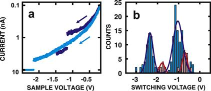
To estimate the electric field strength required to induce switching, the STM tip was positioned above suitable W structures and the feedback loop was disabled. While keeping the tip–sample distance fixed, the voltage was ramped to higher absolute values. Since the W structures only switch to complexes with higher conductance the switching is accompanied by an abrupt increase of the current (figure 8(a)). Occasionally, lateral motion occurred (as verified by subsequent imaging), which leads to a sudden decrease of the current. This experiment was repeated at two different tip heights, which were defined by different currents before opening the feedback loop. A histogram of the switching voltages is shown in figure 8(b), for larger (blue) and smaller (red) tip–sample distances. The starting current for the voltage ramp was increased by a factor of 10 for the smaller tip–sample distance, thus the tip was ≈1 Å closer to the sample. The switching occurred at lower absolute voltages for the smaller tunneling gap, but still at larger currents. This indicates that the process is induced by the electric field rather than the current. As indicated by Gaussian fits there are two probable switching voltages, −1.05 V and −2.35 V (−0.7 V and −1.8 V) for the larger (smaller) tip–sample distance. Assuming a tip–sample distance of 4 Å (larger gap), switching occurred at electric fields of 260 mVÅ−1 and 590 mVÅ−1 which is close to the values obtained for the smaller gap (3Å) of  mVÅ−1 and
  mVÅ−1. This hints to an electric field induced dehydrogenation which becomes likely at a critical field strength. In the case of hydrogenated Co on graphene on Pt(111), the voltages needed to remove H were reported to be somewhat smaller (below 500 mV) [17], possibly indicating that those structures are less stable than the present W–H compounds. However, a dependence of the dehydrogenation voltages on the tip–sample distance was not reported. Dehydrogenation of Ti on hexagonal boron nitride and Ce, La and Cr on Ag(100) was possible at voltage pulses of 4 V [18, 19], but critical tunneling conditions needed to induce this process were not reported.
Figure 8. (a) Current recorded during STM induced switching of two different W structures for the larger tip–sample distance. At constant tip–sample distance the voltage was ramped from small to larger negative values. The switching of the W structures under the STM tip leads to a sudden increase of the current. (b) Histogram of switching voltages, measured as explained in (a), for larger (blue) and smaller (red) tip–sample distances. The continuous curves show Gaussian fits to the datasets.
Download figure:
Standard image High-resolution image
5. Conclusion
In conclusion, we showed that single W atoms on graphene on Ir(111) have a strong affinity to bind H. Unidirectional electric field induced switching (dehydrogenation) between five different W related structures was possible. These structures were characterized by means of STM and STS and assigned to W and WHn, with  . They show a number of peculiar effects, such as electric field induced shifting of spectroscopic features, resonances in the
  spectra, tip induced conformational switching and charging. The complexity of these observations render a theoretical description very demanding but at the same time highly desirable.
Additionally, we showed that H adsorbs at the Ir(111) surface in two different ordered structures at low temperatures, depending on the coverage. These structures can be manipulated by STM.
Acknowledgments
Funding by the Deutsche Forschungsgemeinschaft via SFB 668 is acknowledged.
Footnotes
- 1
The moiré pattern of graphene on Ir(111) does not change upon H adsorption, indicating that H does not intercalate between graphene and substrate. This can also be seen from an Ir(111) surface resonance confined in graphene islands (see figure 5(b)), which is suppressed by H adsorption (see section 3).
- 2